Wednesday, October 27, 2021

Arduino controller VFO/BFO Test Set

I have done several versions of  VFO/BFO circuits using differentmicrocntrolers.  Any of these would work for the Simple SSB transceiver.  Looking at these, you can see that they are also very similar to some of the test equipment I have previously built.  I know that some people who are interested in building this transceiver, have very little in the way of RF test equipment.  So why not build something that can be used to test the modules as they are being built, and then as the Controller,VFO/BFO to finish off the project.

Doing something similar to the test gadget from a couple years ago, I went with a basic Arduino Nano, the SI5351 module, and a TFT Display.  To this I added header pins to bring out pins for a Rotary encoder and other controlls. To an expansion header I brought out  DC power, analog, I2C , and the SI5351 clock lines.  Since some of the TFT Display modules require 3.3 volt logic levels instead of the 5 volt out of the Nano, I added 1K resistors in the control lines to provide current limit for the display if using a 3.3 v module.  

This also helped make the layout a little easier.  After a number of tries I was able to get the layout to fit on one of the 50 x 70 mm perfboard in the kit I purchased.  When building this module I found that it worked quite well to bring the wired up from the bottom of the board and run them across the top and back down to connect at the other end.   Doing this kept the board fairly neat.  The only insulated jumpers I had to install were to bring the 5V line across the expansion header. This layout would also work well for etching or routing a single sided circuit board.

After building the board, the only thing I had to do to one of the early Arduino sketches I had for a simple VFO/BFO was to change a couple pin definitions for the SPI lines going to the TFT display.  This made a fairly compact board that can be easily mounted, with a connecting cable going to the rotary encoder and several switches on the control panel.

Since I also want to be able to use this as a test_set during construction of the RF stages. I built up a small board with a rotary encoder and 3 push button switches that plugs on to the control header pins on the Arduino controller board. 

 Looking back at the Sweepering Jr., and different versions of the SNA Jr. projects, I decided to go with much of the original SNA Jr. design.  I built a simple add on module that can be used as a Sig.Gen., SNA, RF voltmeter.

I bring out two of the SI5351 clock outputs throughs DC locking capacitors, one of them has a 50 ohm load placed across the output.  This can be used as a two channel signal generator. There is limited level control, but you can build  very simple attenuators to take care of that issue.  Instead of using an AD8307 Log amplifier for RF measurements, it used a 1N60P shunt diode detector feeding a MCP6002 operatinal amplifier.  This two channel op-amp is very nice to work with in microcontroller circuits.  It only requires a single ended power supply, and works well at 5 volts.  It has rail to rail output, so you can use the whole 5 volt input range of the Arduino Nano.  They are readily available in 8 pin DIP and SMD versions, and are less than $1 through most suppliers. This circuit does not have the sensitivity or dynamic range of an AD8307.  But, for use as a RF voltmeter or in a SNA over the range of voltages expected in testing the transceiver it will be very adequate.  One of the detectors has a 50 ohm load on the input for power measurements or use as an input for the SNA function.  The other is configured as a remote RF probe with a x1/x10 voltage divider, for basic RF level checking.   

Just like other parts of the project,
the test set options will be built as simple modules. The test set modules will plug onto the 18 pin expansion header on the VFO/BFO board.  It is built on one of the 50x70 mm. boards in the kit I purchased.  You can use edge mount SMA  connectors for all, but I substituted 3 pin right angle heder pins for the RF probe connection, so I could use it for other possible functions. A 3 pin keeps the layout the same for either, and makes a more solid feeling connection. 


 Adding an adapter board for the TFT display and making a simple 3D printed sleve to hold everything, the modules plugged  together make afairly compact test set.  

Now to finish the software.  It will have parts from the SNA Jr., 2 channel signal generator, and Sweeperino Jr. projects, plus a couple more if I can fit them all in the Nano.

 I hope to have several other modules that such as an antenna nalyzer. SWR power meter. measurement receiver, and possibly a very simple Spectrum Analyzer for up to about 60 MHz.  These will be added as the transceiver project progresses.


Wednesday, July 28, 2021

Testing Audio Amplifiers

 After finishing the microphone amplifier and the AF amplifier modules, it is time to test them.  For the experienced builder with  scope and signal generator available it is no problem.  If you are new to building, and don't have these available, there is a very inexpensive option that may even work better.  

I spent more than 25 years working as a field service technician.  During this I spent more time than I want to think of dragging scopes, and other pieces of test euipment around.  During the last years before I retired, I found several useful pieces of software that allowed you to use PC sound cards as scopes and or signal generators.  Although they were not suitable for calibrating the equipment I worked on.  They were more than adequate for trouble shooting, and verifying   basic system operation

New-Mini-USB-2-0-3D-Virtual-12Mbps-External-7-1-Channel-Audio-Sound-Card-Adapter

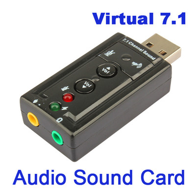
Although these worked better with actual sound cards, they also work quite well with the very inexpensive USB sound cards that are available simular to this one. 

 Other USB sound cards will give more options such as dual channel input, but are more expensive. 


Only prblem I have found with the USB card is that sometimes there are higher frequency signals found because of traffic on the USB bus.  This has normally been  higher than the 5 KHz. I think of as the upper limit for frequency response in comunication equipment.

They only requite a simple interface to provide usable results. I have tried several, from basically just  DC blocking capacitors,to ones with internal amplification.  

The one I use most of the time uses a simple X1, X10 voltage divider along with DC blcking capacitors on the output to the MIC input on the sound card.  If you use an internal sound card with a Line Input, you can build a two channel version of the interface. 

If you use Line Input you can  elminate the DC blocking capacitor going into the sound card. It is there to remove the DC voltage out of the MIC input used to power Electoret microphones and provides protection for the sound card.  I like having some protection for the sound card from DC voltages in the circuit being tested.  Espically if you use this to test Tube circuits, with their higher voltages.  To add this place a pair of back to back diodes 1N4148 orsimilar across the input to the sound card to ground.

For the  Signal generator output, I capacitivly couple the sound card stereo channels to a 1K pot.  This couples the L and R channels , and lets you ballance the output levels so you can use this to generate a two tone audio signal for testing transmitter out settings. The combined output then goes to a Pot. for level adjustment and a DC blocking capacitor to the output connector.


This is also built with perf board, and use right angle header pins as output connectors.  The header pins let me use JST jumpers to connect to modules being tested or to build simple fixtures for making testing easier.   Instead of a switch I use a 3 pin header and jumper to selecdt voltage level.  You could also replace the voltage divider with a 1 Meg. Pot. to make construction even easier.  I used some 3.5 mm. jacks for the signals going to the sound card.  You could elminate them and use a 3.5 mm stereo cable cut in half and wired directly to the circuit.

There are two different software packages under Windows 10 that I use.  One is Soundcard Oscilloscop    and the other is Visual Analyzer.

They have similar basic functions 

    2 channel scope with XY display

    FFT based frequency spectrum display

    2 Channel signal generator

Visual analyzer has additional functions among them a Voltmeter, Frequency Meter, with additional hardware a ZLRC meter.  
Both free for non commercial use, a commercial license or donation available.

I am only going to use Soundcard Oscilloscope for this post.  After doing the install you get the main screen.


Functions are selected from a set of tabs above the scope display.  First thing you need to do is select your input and output device,  and set the scope paramateurs.  Amplitude calibration can be done later. For ease of learning the interface select scope loopback for input and output device

First function  to check out is the  Oscilloscope function selected by clicking on the first tab.  To the right you have controls for setting the voltage range per channel and the timebase for the sweep.  There are also options for setting trigger type , slope, and threshold.  

Just below th display area there is a button to set the type of measurement you can make.  You can set cursors for both amplitude and time. For both there is a display value for the reference cursor and the difference between it and the second.


The next thing to look at is the
signal generator tab.  This allows you to select the type of signal generated, frequency and amplitude for each channel.  It also allows you to set up frequency sweeps that are very handy for checking frequency response of amplifiers. This can be brought out as a separate window to make it easier to use.

The last function I commonly use is the frequency display.  This uses a FFT to compute a spectrum display of the input signal in the frequency domain, instead of the time domain.  This is very useful for measuring the frequency response of a audio  amplifier or filter, when used with the signal generator.  You can place a cursor on a signal  to get the frequency of the signal. Along with the cursor you can use the zoom function and position to look at a signal in more detail. Unfortunatly there is no vertical cursor, so you have to turn on the grid and reference signal levels to a scale on the side. Some of the other useful options in this function is the ability to look at the levels in dB, and usea peak hold when sweeping to plot the frequency response of a amp or filter.

One common way to check frequency response, is to set the signal generator start frequency, turn on sweep and set the end frequency and sweep time.  I usually set the end frequency to about twice the highest frequency response I am trying to measure.  Then on the frequency display set peak hold and set to dB and auto scale.  Let it run a few passes and you have a good indication of the frequency response of the amp or filter. Do this with two different signal levels and you can find the gain or loss of the device being tested.
Another method to measure frequency response is to select White Noise as the signal being generated.  On the frequency display panel everything is set the same.  After a few passes the frequency response shold be clearly seen.  Make sure you use White Noise and not Pink Noise.  White Noise has a  constant amplitude over the whole audio frequency range, where with Pink Noise  the amplitude fall off as frequency increases.  For checking frequency response it can show a incorrect result at higher frequencies.


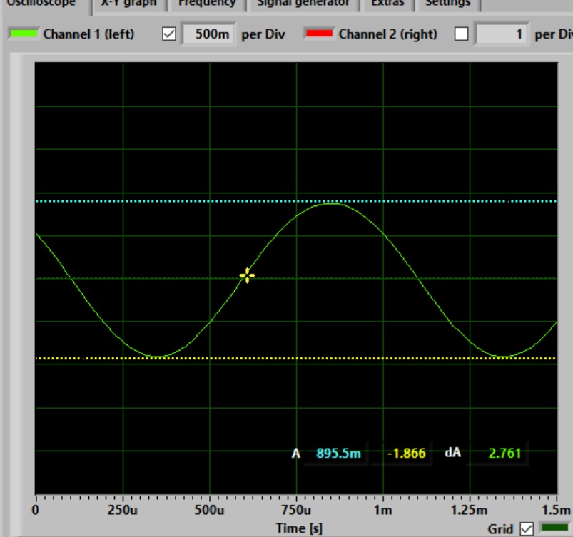
Now lets switch to the sound card input and output, and connect to the microphone amplifier.  After setting the signal to a 1KHz Sine wave and a level  just before the output started to distort.

 I switched to the frequency mode and set the signal generator to sweep from 20HZ. to 20KHz. With the display in dB and max hold, you can see the frequency response is flat from 100 Hz to over 10KHz. 
 The log display makes it look noisier at the higher frequencies. But, if you look at the response you see that the noise level is fairly constant across the whole range.

There is one alignment of the test fixture that should be made, that is to adjust the balance between the two channels.  This signal will be used later to do a two tone test for setting the microphone level.  A good Youtube video by W2AEW  Two-tone test of SSB transmitter output explains the test quite well.  The two frequencies should be non-harmonically related and adjust the balance for equal levels. I used 750 and 1250 Hz. and set the cursor at 1000Hz.  Then use the zoom control to spread the traces apart.  Then just adjust the balance pot for equal amplitude.  Make sure you have peak hold turned off while doing this.

Testing the audio amplifier module is the same as the mic. amplifier.   Only thing different is that you need a load between 4 to 32 ohms on the output. The first stage of the audio amp. is nearly identical to the mic. amp., it is followed with a LM386 AF amp IC.   The volume control should be a audio taper pot, but I only had linear taper in my parts box.  You can approximate an audio taper by adding a resistor between the wiper and ground terminals on the pot.  You need to use a larger value pot. to compensate for the final parallel resistance.  Normally the added resistor value is around 20% of the pot. value. I ended up using a 20K pot and a 3K9 resistor.

Setting things up the same as for the mic. amp., 1 KHz. sine wave set the input level and volume control to just below the point of distortion on the output signal. This is kind of tricky because of the gain of the LM386 is set quite high and you can get the output to distort very easily. I turned on the  sweep from 200 Hz. to 20 KHz. and let it run for a while with peak hold turned on. I got a linear response from 200 to just over 8 KHz. where it started to drop off a little. Overall the AF stage has quite a bit of gain, that can start to distort fairly quickly, but has a flat response over the frequency range of interest for communications equipment.  Gain on the LM386 can be reduced by decreasing the value of th capacitor between pins 1 and 8 of the IC, if desired. 
Thats it for testing audio amplifier stages.  AF filter response can be tested iin the same way. 

 Next I will work on the VFO-BFO oscillator, based on a SI5351 module and Arduino.  I have done several versions of these before, but will layout a simple version that can easily be built on the same style perf boards.  I plan on bringing pins out that will allow the module to be used for testing RF stages in the transceiver. Hopefully I can get this to work similar to the original SNA Jr. or Sweeperino from my earlier posts.  This should be very helpful for those  who do not have anything in the way of RF test equipment.


.

Thursday, June 24, 2021

Simple SSB Xcvr Mic Amp build & AF amp layout

 I had decided to build most of the transceiver using perf board.  I prefer the double sided plated through hole variety to the bare variety.  For me it just makes it easier to solder the part in place, and then route the leads as needed.  Also if you have to replace a part, you can usually just  clip it off on the top and solder in a replacement without changing the connections on the bottom. 

This type is available in various sizes. You can find small kits with several small sizes for around $10.  You can also get larger size boards and cut to the size desired.

After I received the kit, I changed the layout to fit one of the sizes in the kit.  The extra time spent making an exact layout template really saves time, and frustration in the long run.  I also did the layout in ME Pad  and Muppet format, and all are available at

https://www.dropbox.com/sh/v9rr5cqg9a788qe/AADuZN4t4wCLGh8orBzdFUwTa?dl=0

When I first started building some of my projects, I used many components I had salvaged from junked equipment, or surplus supliers.  Anyone remember 'PolyPacks' ?  Because of this I got into the habit of always measuring the value of the components as I used them. Time spent doing this also paid for itself many times over.  Now I use better quality parts, but still test them before use.  Getting harder to read the values on these small parts for some reason. 

For this I use one of the inexpensive component testers available through the usual suppliers. The one usually use is similar to this one, and has pads for use in testing SMC components.  They are available with or without cases for $10 - $20.  Most of them measure R,L,C, along with diodes, transistors and FETs.  For the seimconductors, they give pinout along with values such as gain and internal capacitance depending on type being tested. The first one I bought did not have a case so I found the design for a 3D printed one.

Following the template, it only took a little while to do the actual construction.  For audio and  digital boards I use either straight or right angle header pins for connectors.  This allows me to use JST style jumpers for wiring for DC and control signals.  You  can also add connectors to shielded cable if needed.  Or, you can easily solder wires directly to the pins if desired.  For much of my test gear, I have adapters made up so I can use JST jumpers for ease of testing modules.

Now that this module is finished, I did a layout template for the AF amplifier.  Since the premap half of the AF amp is nearly identical to the Mic amp, I could just move components over a little to make room for the LM-386 and associated components. 


It turned out like this. This was fairly crowded on this size board, so I did another template using a slightly larger board in the kit.  This one allows plenty of room for components.  Either version will work.  Just up to the builder to choose the one they prefer.

I also did a ME Pad template for those that like that construction method. but only for the smaller size board.  They are available at

https://www.dropbox.com/sh/ia55ghqyibs5iur/AAAlbEp8ARKuvKQ38VONz5zMa?dl=0


Next time I will have the AF Amp board finished, and will describe the simple test gear and software I use for checking audio frequency stages.


Thursday, May 27, 2021

Simple SSB Xcvr Mic Amp layout


Normally I would start with the audio amplifier board, but in this case I will start with the microphone amplifier for two reasns. First it is the simpelest to build, and second almost all the other circuits in the transceiver are just a variation of the same common emitter amplifier. Values have been changed to provide different gains, or frequency response. For the RF stages. compnents have been added to provide impedance transformation to make it easier to connect to the next stage.  If you look, the bi-directional amplifiers in the IF stage are basically two common emitter amplifiers on top of each other. Switching  power to the desired amplifier changes the direction of signal flow.
The schematic and values are directly from the LT Spice simulation by Pete, with the exception of an added 100K resistor that can be jumpered in if you need to power an electoret micrphone.  For a lot more informationon how the values are determained check this YouTube by Charlie  ZL2CTM on Common Emitter Amplifier design  If you have not already checked Charlie's YouTube channel you are missing out on a huge amunt of information.  He has built a variety of both hardware and software defined radios.  He goes into the the math required for the design in a lot more detail than I even want to think about.

I have tried many different construction methods over the year, and have found that time spent doing the inital layout, can save much more time and effort in the actual build.  I have tried 'Ugly' or 'Dead Bug' , I find that it quickly turns into something that is impossible to modify if necessry. At least for me, I have seen some fantastic builds that others have done. I perfer using a Perf-board for one off AF or RF circuits, and for almmost all Digital circuits.  

I started just doing the layout with pencil and paper, but still ended up running out of room or needing to use a lot of jumpers.  A few years ago I started using PCB design software, and now use it no mattr what method of construction I will be doing.  There are two main types of PCB design software.  One ties the PCB layout directly to a schematic. This offers more assurance that the layout will be correct according to the schematic.  The disavantage is that if you want to make a change to a component or value on the layout you will have to go and make the change in the schematic first.  The other type is more of just a graphic design program that allows you to add or change components in the layout as you want.  This means that the entire correctness of the layout is up to you.  

But depending on the software, this method has some major advantages. The software I usually use allows me to take part of an existing layout and save the entire section as a component in the library.  Most of the other programs I have tried allow you to make new components, but will not allow you to save a part of a layout as a component. 

One of the design programs sometimes I use is ExpressPCB+.  It is free but tied to a single board house.  You do not have to option to export as a Gerber file that can be sent to any PCB house.  For those who make their own PCBs using the toner transfer or other metods can use the printed output of the program to make the transfer image. My favorite proram is Sprint Layout, not free but only around $50. It has all the options of ExpressPCB+, and the ability to generate Gerber files along with many other features.

First thing I do is design the board as if I was going to make a simple through hole PCB. I can easily move components around to fit the size board I want, simplify layout, and elminate as many corssing lines as possible.  I could generate the image to use for toner transfer and etch a board, use a cnc router to mill the board  If I set the grid size to be .1" (2.54mm) I can use it as the layout template for a perf-board build.   They will look something like this.  

For RF and digital circuits it is often desired to have a large ground plane on the board.  In this case the software allows you to fill the board with a copper pour, and isolate the traces and component pads that are not connected to ground.  This can be either etched or isolation routed.  In this example I show the  ground trace just as reference, It is really through the copper pour that the grounds are connected.  On more complicated boards this can be a problem if component and trace layout isolate ground from one area of the board to another.  In this case jumpers may be necessary, or a double sided board with 'vias' to connect the ground sections together.


These two examples use through hole components, and for the hobbiest that  means a lot of drilling.  To make this simpler for the another method called 'MUPPET' has been developed.  this moves the copper traces from the bottom of the board  to the top.  Instead of pads around the through holes, a large solder pad is placed at the end of each component lead.  It is fairly easy to bend the component lead sso it can be soldered to the board.  Ground connections go directly to the copper .


For those who do not want to take itme to etch boards, another method called the 'Manhatten Method' is very common.  It uses small pads made from copper clad circuit board gluded to a piece of bare copper PCB material.  These pads may be home made, or a commercial product called 'ME Pads' are available.The things you have to watch for is that any adjoing pads are properly jumpered, and that connected pads should be jumpered with insulated wire to prevent shorting to the  ground plane. This method has the advantage of being very quick and the template looks something like this.

Another common method used is to create 'islands' on the bare copper PCB material witha CNC router, or manually by using a tool such as a 'Plexiglass cutter' to scrape lines through the copper PCB material. The most important thing if done manyally is to make sure all the copper material is cleared away, and there is no connection between the islands.   This could also be etched if desired.   Again the traces are shown only for reference, the components are soldered directly to the PCB 'islands'.

From these simple examples, you can see that the same layout can be used as a template no matter which method you want to use.  There are several other methods using things like strip boards that are used by very successful builders . Look around on YouTube, and you can get more information on many of these methods.  Some of my earlier posts cover toner transfer PCBs and might be helpful. 

So no matter what method you want to use for the project, my reccomendation is to play with the layout using whatever PCB design program you want and simplify the layout as much as possible before you heat up a soldering iron.

Now I have a useable template for a perf-board version, and a package of parts just arrived yesterday so I can get started on the mic amp.  Next post will look at how it is built and some simple ways to test it and the AF amplifier module that comes next.


Friday, May 14, 2021

The N6QW Simple SSB Transceiver

 Those that have been following my blog for a while, know that I am a fan of  Pete Juliano, N6QW, and his MANY transceiver projects.  Recently on the SolderSmoke blog, there was a post about one of Pete's project being built by group of amateurs belonging to the Vienna Wireless Society in Virginia.

http://soldersmoke.blogspot.com/2021/04/homebrew-lives-twenty-n6qw-simple-ssb.html

 A member of my local QRP club posted this to our groups.io page, and there were several people that were interested in building one. I contacted Pete, and he put me in touch with Dean  KK4DAS.  Dean is the one  leading the group at VWS through the construction of around twenty  SSB transceivers.  As of now almost half of the group have their project up to a working receiver.

The other evening I was able to join their group in a Zoom meeting. They went over their progress. and shared information on the next stage in the build.  I have also spent a lot of time going through the documentation they have been creating on the VWS Makers Group SimpleSSB Project page.  Some of the information there covers the module layout they used, some simple test equipment needed, and  software developed.  Dean has added to the oritional software, to provide support for different display types, and added features like CAT control.

Several of the members of my local club interested in this project have only experience building some of the kits available through the common QRP sites.  They feel that they would need quite a bit of detailed information to build something from just parts.  I decided I will start working on a series of blog posts that will document the build in a detailed way that can  fairly easily be copied by someone with very little or no experience.  I know that most of these members have very little in the way of the test equipment that would be helpful in a project of this type.  In these posts I also plan on describing some very inexpensive or easy to build test equipment. And, I plan on adding  some test functions into the transceiver itself.  A lot of the test equipment information will be a reference to or revisions to what I have covered previously in this blog.

Most of the design is based on the work of Pete N6QW  and can be reffenced at the links in his blog.  N6QW.BLOGSPOT.COM

Some of the minor mods I have made are based on some of the things I learned watching Charlie Morris ZL2CTM YouTube Videos.  For those who have not seen any of Charlie's videos, he goes through in great detail the math involved in the design of his circuit design.  Also incorporating the info from Dean and the VWS group, and some of my own ideas and preferences.

There are several options commonly used for buildiing a project of this type.  Manhatten or MePad, Perf-board, CNC Routing, and the one I use quite a lot Toner transfer etching. For this I will use perf-board for most of the modules.  My preference is using double sided boards with plated through holes.  There are several inexpensive kits available with an assortment of sizes for a  very reasonable price.  These small boards are ideal for building individual modules. The probem many new builders find is getting the layout so it is easy to build.  I perfer to use a PCB design program with the layout grid set to the .1" of the perf-board.  This makes it easy to move things around  to get  a nice neat layout that is easy to duplicate.  Then it is easy to transfer this to the perf-board for the actual construction.  With this layout I can also generate files for Toner Transfer etching, or CNC routing.  Even Gerber files if one desires to have boards made by one of the inexpensive board hoses in China.

These are my plans for the next few posts.  If anyone else would be interested in this project contact me directly at duwayne@kv4qb.us.  With most people now familiar with Zoom and Jitsi meetings, it would be possible to schedule meetings for everyone to get together and work as a group.

Not I need to go check my parts bins and see what extra stuff  if any I need to order.


Tuesday, February 23, 2021

Instrument storage boxes updated


While getting some equipment off a shelf I knocked some thing down and they landed on a nanoVNA, cracking the screen.


I think it is time to make some protetive cases for the equipment when not in use. Looking around on Thingiverse I found a small case that is similar to to a Pelian Case.  I printed one and fund it to be exatly what I wanted.  It is very strong with a nice latch system that closes very tightly.  It has a seal that can be made watertight if I run a small bead of silicon tub sealant in the grove in the bottom part of the box. Or there is a seal that can be printed using flexible filament.

Using this basic design and dimensins for the hinge and latch mounts, I designed several more boxes of the sizes I need for some of my other instruments. With this design I can  use the same lacth and hinge parts as the original design. 

I printed these up using some HIPS, PLA or PETG for the case top and bottom. These all worked quite well, with the PETG probably providing a little tighter seal.   I found that PETG worked best for the hinge and latch parts.  Since it is slightly flexible it holds the two parts of the case  tighger than ones I printed with of PLA.

I lined the inside of a case with some mediam density foam to hold the instruments in place and provide quite a bit of protection.


I am going to try to design some printed inserts for some of my other instruments instead of making them out of foam.

After I clean up some of the cad fies I will post all of then for anyone interested.

Original box design on thingiverse 
https://www.thingiverse.com/thing:4094861
Use the latch and hinge components for all other designs

Update

Designed and printed a new box bottom for a NanoVNA.  This has built in compartments to hold the VNA , cables, and cal standards. I use connector savers on my VNA, so had to make the compartment a little longer.  This gives me room to also store my printed torque wrench.  Will have to print one for my other nanoVNA.  With a piece of foam in the topccover, everything stays in place.


 Still need to play with some of the printer settings.  So far it looks like I need to use about 15% simple grid infill to keep the weight down.  And 3 perimiter layers and 5 top and bottom layers.

Still checking and cleaning up the CAD files.  Since I am using a fairly old commercial CAD program that does not use a standard file format for the raw file I will be exporting them to .stl format.  As I check the CAD files I will store the .stl to this dropbox folder.

https://www.dropbox.com/sh/5culi2oajisapdr/AAB_u4oxVUge0kJR0sVSVp3Ra?dl=0